For decades, the semiconductor industry has followed the trajectory of Moore's Law, shrinking transistors to pack more power into smaller, faster, and more affordable chips. But as we approach the physical limits of silicon scaling, a new paradigm has emerged as the path forward: Heterogeneous Integration (HI), powered by the rise of chiplets.
This shift is more than an upgrade — it’s a transformation in how high-performance silicon is conceived, designed, and manufactured. It’s also essential for the next generation of compute-intensive applications, from cutting-edge AI accelerators to exascale supercomputers.
The Limits of Monolithic Design
Traditional System-on-Chip (SoC) designs have aimed to place every major function — CPU, GPU, memory controllers, and I/O — on a single, monolithic die. While powerful, this approach comes with several critical drawbacks:
- Yield Issues: A single defect on a large die can fail the entire chip, raising manufacturing costs dramatically.
- Design Complexity: Integrating many different functions on a single process node often forces compromises, especially when mixing analog, RF, and high-speed digital logic.
- Rising Costs: Creating large monolithic chips on advanced nodes is increasingly expensive and risky.
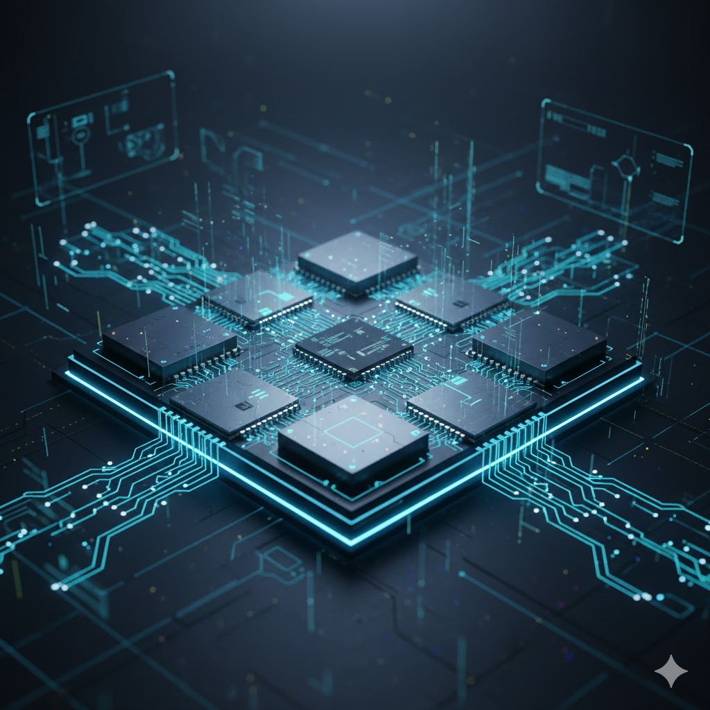
Enter Heterogeneous Integration and Chiplets
Heterogeneous Integration brings together multiple smaller components — chiplets — each fabricated separately, into a unified package. This “system in a package” (SiP) approach allows designers to combine CPU chiplets, GPU chiplets, memory chiplets, and other specialized functions, each built on the most suitable process technology.
The Game-Changing Benefits of HI
Moving from monolithic SoCs to chiplet-based architectures unlocks a long list of advantages:
- Optimized Performance & Cost: Each chiplet can be manufactured on its ideal node — cutting-edge for compute logic, mature nodes for I/O — balancing power and cost.
- Improved Yields: Smaller dies have higher yields. If one chiplet is defective, only that piece is discarded, not an entire costly SoC.
- Scalability & Flexibility: Chiplets can be mixed and matched like building blocks to create custom configurations. Need more compute? Add additional CPU chiplets. Need more bandwidth? Integrate HBM memory stacks.
- Power Efficiency: Shorter interconnects and optimized design reduce power consumption compared to large monolithic chips.
- Reticle-Limit Bypass: Chiplets sidestep the physical size limits of a single reticle, enabling extremely large compute solutions once impossible with monolithic designs.
Tecknoz: Pioneering Designs for the Chiplet Era
At Tecknoz, our ASIC/SoC Design and IC Layout teams are actively engineering solutions for the chiplet-driven future. We deeply understand the architectural and physical challenges of Heterogeneous Integration, including:
- Building robust chiplet-to-chiplet communication interfaces such as UCIe and AIB.
- Optimizing thermal management and power delivery for advanced 2.5D/3D stacked architectures.
- Developing high-density interconnect strategies for next-generation packaging technologies.
Through our expertise, Tecknoz helps clients fully leverage chiplets and HI to achieve top-tier performance, power optimization, and cost efficiency in their semiconductor products.
Ready to integrate the future into your silicon? Partner with Tecknoz.